Overview
The Goal
Master AI inference, AI agent harness systems, and hardware engineering — then design a physical AI chip.
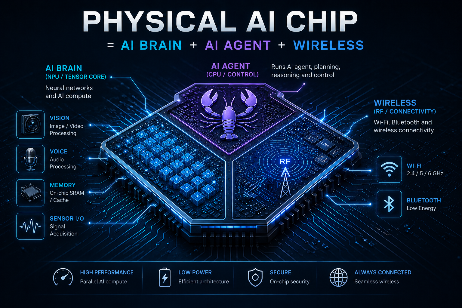
The endpoint is a single die that runs production AI workloads, hosts a real agent runtime, and talks to the physical world over Wi-Fi/BLE/Thread — a Jetson-class AI brain fused with an ESP32-class wireless stack on one chip. Designing it takes three working skill sets at once: inference engineering (Qwen-class decode, kernels, quantization, rooflines, multi-GPU serving), agent harness systems (sessions, tools, multi-agent loops, RAG, evals, production observability), and hardware engineering (RTL, embedded Linux, Jetson, ESP32, RF, ASIC flow). This roadmap teaches all three side by side — the chip is the artifact, but the three pillars are the actual work.
The Three Pillars
                          ┌──────────────────────────────────────┐
                          │      Physical AI Agent Chip          │
                          │   one die  ·  Jetson + ESP32 fused   │
                          │   AI brain + wireless + sensors      │
                          │   + agent runtime — ships in product │
                          └────────────────┬─────────────────────┘
                                           │
                  ┌────────────────────────┼────────────────────────┐
                  ▼                        ▼                        ▼
         ┌──────────────────┐   ┌──────────────────┐   ┌──────────────────┐
         │   AI Inference   │   │   Agent Harness  │   │     Physical     │
         │   Engineering    │   │     Systems      │   │     Hardware     │
         ├──────────────────┤   ├──────────────────┤   ├──────────────────┤
         │ GEMV/GEMM        │   │ Agent runtimes   │   │ Digital design   │
         │ Quantization     │   │ Gateways/RPC     │   │ HDL → ASIC flow  │
         │ KV/paged attn    │   │ Skills & tools   │   │ Computer arch    │
         │ Multi-GPU TP/PP  │   │ Multi-agent loops│   │ Embedded Linux   │
         │ Rooflines        │   │ Observability    │   │ Jetson (AI brain)│
         │ Real models      │   │ Production SDLC  │   │ ESP32 (wireless) │
         │ (Qwen3, 72B…)    │   │ OpenClaw, SDKs   │   │ Sensors / ISP    │
         └──────────────────┘   └──────────────────┘   └──────────────────┘

           ┌─────────────────────────────────────────────────────────┐
           │ Convergence on one die:                                  │
           │  Jetson NPU/GPU/DLA  ─┐                                  │
           │  ESP32 Wi-Fi/BLE/    ─┼──► Physical AI Agent Chip        │
           │   Thread/Zigbee       │   (your tape-out target)         │
           │  ISP + sensor MIPI   ─┘                                  │
           └─────────────────────────────────────────────────────────┘
1. AI Inference Engineering
The workload your chip will run. You learn how decode is bandwidth-bound, how GEMV/GEMM kernels actually dispatch, how K-quants work, how to size a roofline, how to optimize Qwen3-4B on a Jetson and Qwen2.5-72B on 4×H100 — so when you design silicon, you know exactly what bytes-per-token your accelerator must move and what tile sizes the compiler will hand you.
2. AI Agent Harness Systems
The software stack that lives above your chip. Agentic runtimes (OpenClaw, OpenAI Agents SDK), session models, gateway RPCs, tool calling, skills, multi-agent loops, evals, observability. A physical AI chip is the substrate that runs harnesses like these in a battery-powered product — knowing how they behave tells you which inference patterns to optimize for, what wake-on-event the radio block must support, and what state your boot ROM has to preserve.
3. Physical Hardware Engineering
The substrate itself — both halves of it. The AI brain (digital design, computer architecture, CUDA, Jetson Orin platform work, custom carrier boards, L4T, TensorRT/DLA) and the wireless stack (ESP32, OpenThread, Zigbee, ESP-Hosted, RF integration). Plus the embedded Linux, RTL design, HLS, and AI-chip-design specialization that puts NPU + radio + ISP + Linux on one die. You don't get to a tape-out without standing on both halves of this stack.
Why the combination? A chip without a runtime is a brick. A runtime without an agent stack is a benchmark. An agent stack without inference cost discipline is a demo. An inference accelerator that can't talk to the world over Wi-Fi or BLE is a coprocessor someone else has to integrate. The three pillars are how you build a chip that ships in a real physical product — at the workload, the runtime, the radio, and the silicon at the same time.
What You'll Have at the End
The reason for this roadmap, written as a checklist:
- You can take a transformer model, predict its decode tok/s on a given chip from first principles, and explain where it falls short of the roofline.
- You can hand-tune a CUDA/kernel path for a Qwen-class model — fused QKV, fused gate+up, CUDA Graphs, INT8 KV, speculative decoding — and quote a before/after benchmark.
- You can run a production agent harness end-to-end: gateway, sessions, skills, tool calls, multi-agent supervision, observability dashboards, the lot.
- You can take a Jetson module, design a carrier board for it, bring up custom L4T, flash it in volume, and ship a product against FCC/CE.
- You can bring up an ESP32 wireless coprocessor over SPI, expose it to a Linux host as a Wi-Fi/BLE/Thread/Zigbee radio, and integrate it into the same product.
- You can write RTL, drive timing closure on a real FPGA, and lower a small transformer block through HLS or a custom MLIR dialect.
- You can write the architecture spec for a physical AI agent chip — one die containing an NPU tile (Qwen-class decode at edge power), a wireless subsystem (Wi-Fi 6/BLE 5/Thread/Zigbee), MIPI CSI-2 camera input, ISP, audio I/O, and a Linux-capable CPU — with realistic numbers for tile size, SRAM budget, MAC array, DMA, RF integration, and compiler/runtime interface.
That last bullet is the goal. The first six exist to make it real.
Who This Is For
- AI/ML engineers who want to stop treating inference as a black box and design the chip that runs it.
- Inference engineers who want to extend up into agent-runtime co-design and down into kernel + silicon.
- Embedded/firmware engineers who want to climb the stack — from boards to runtimes to chip architecture.
- Hardware/RTL/FPGA engineers who need workload and runtime intuition before specing accelerators.
- CS students who want a structured path that ends at "I designed a chip" rather than "I read about chips."
If you only want to call an LLM API, this isn't for you. If you want to design the silicon that calls it, keep reading.
The AI Chip Stack
Everything in this roadmap maps onto an 8-layer stack. The point isn't to memorize layers — it's to understand how decisions in one layer ripple through the others.
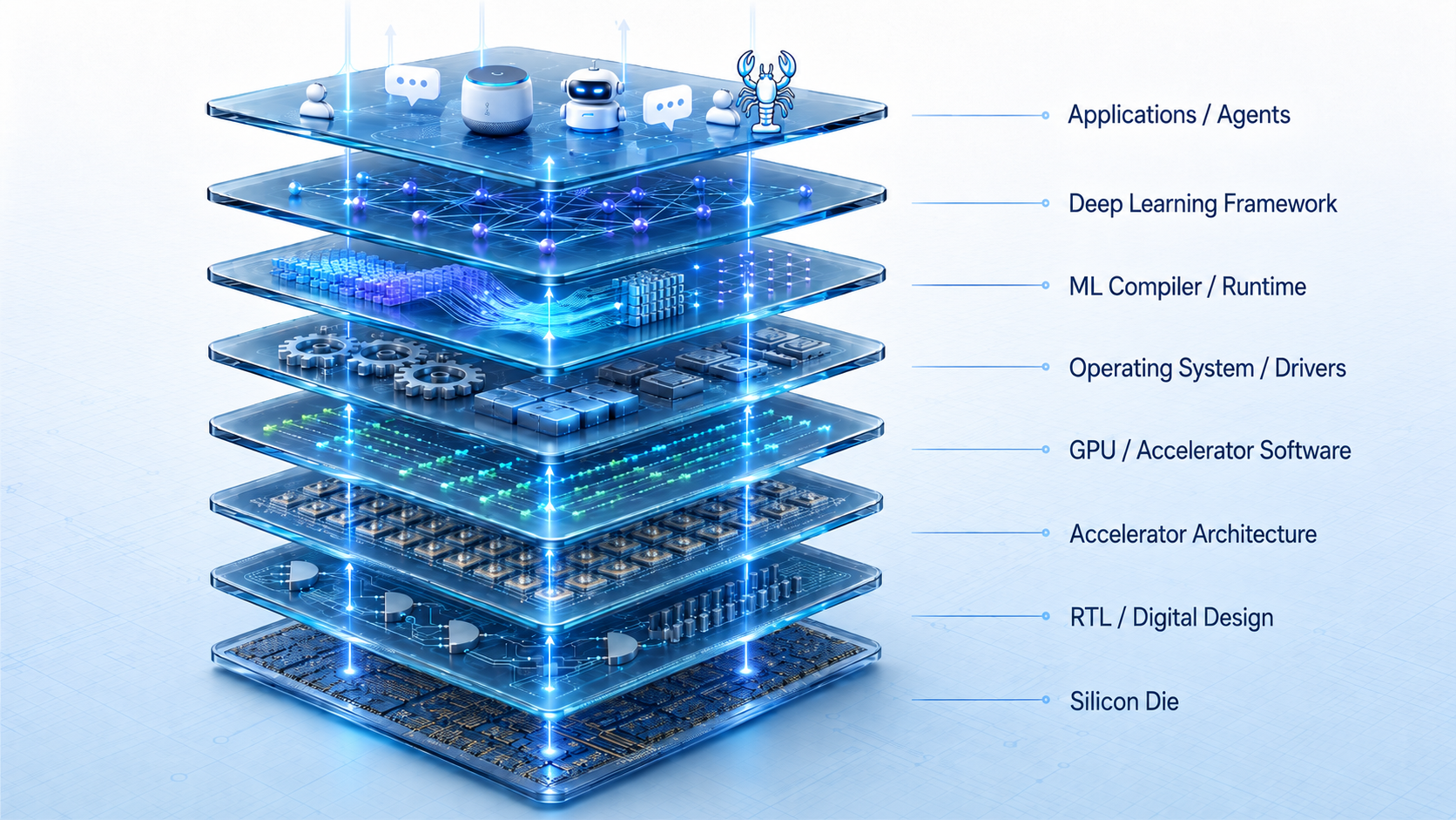
When you're designing a chip, every layer is a constraint and a degree of freedom. The roadmap teaches you to read the whole column.
The Path
Five phases. The first four are foundation; the fifth is where the three pillars converge.
Phase 1 — Digital Foundations (Hardware pillar)
The language of hardware. Logic gates → GPU code.
| Module | What you'll learn |
|---|---|
| Digital Design & HDL | Verilog/SystemVerilog, simulation, the language you'll later write your accelerator in |
| Computer Architecture | CPUs, GPUs, caches, memory hierarchies — the mental model behind your chip |
| Operating Systems | Processes, drivers, scheduling — what your chip's host actually does |
| C++ & Parallel Computing | SIMD, OpenMP, CUDA, ROCm, OpenCL/SYCL |
Phase 2 — Embedded Systems (Hardware pillar)
Get hands-on with real hardware. MCUs, sensors, embedded Linux.
| Module | What you'll learn |
|---|---|
| Schematic & PCB Design | Read schematics, design carrier boards |
| Embedded Software | Cortex-M, FreeRTOS, SPI/I²C/CAN, IoT (OpenThread, Zigbee) |
| Embedded Linux | Yocto, PetaLinux, driver bring-up |
| Product Design | Going from prototype to shippable product |
Phase 3 — AI Workloads (Inference & Agent pillars start here)
Understand the workloads your chip must serve. Core + two tracks.
Core (everyone): - Neural Networks — backprop, CNNs, transformers from first principles - Transformer Fundamentals — the prerequisite for every inference lecture downstream - Deep Learning Frameworks — micrograd → PyTorch → tinygrad
Track A — Hardware & Edge AI: Computer vision, sensor fusion, Voice AI, Edge AI & optimization. Feeds Phase 4B and Phase 5C.
Track B — Agentic AI & ML Engineering: 42 lectures on agent harnesses, LangGraph, multi-agent systems, RAG, evaluation, production runtime discipline, OpenClaw, OpenAI Agents SDK, security, plus a Qwen3.5-4B-Base Unsloth fine-tuning course. This is the agent harness pillar in its primary form — read in order if your destination is the chip + runtime + harness story.
Phase 4 — Deployment & Compilation (All three pillars co-exist here)
Take AI to real silicon. Three specialized tracks.
| Track | Focus | Pillar |
|---|---|---|
| A — Xilinx FPGA | Vivado, Zynq MPSoC, HLS, driver dev, video pipeline | Hardware |
| B — NVIDIA Jetson | Orin platform, custom carrier, L4T, OTA, TensorRT/DLA | Hardware + Inference |
| C — ML Compiler | MLIR, TVM, Triton, kernel engineering, quantization | Inference |
You don't have to do all three. But to land at chip design, you want enough of A to write RTL, enough of B to know what an inference platform looks like, and enough of C to know how a compiler will target your chip.
Phase 5 — Specialization & Convergence
The three pillars converge here. Specialization tracks plus the chip-design endpoint.
| Track | What you'll specialize in | Pillar(s) |
|---|---|---|
| A — GPU Infrastructure | Multi-GPU, NVLink, NCCL, AMD ROCm/HIP, MI300X | Inference |
| B — HPC (CUDA-X) | cuBLAS, cuDNN, NVSHMEM, 40+ libraries | Inference |
| C — Edge AI | Holoscan, Edge LLM Inference Internals, Qwen Inference Optimization (6-lecture series), AI-driven wireless | Inference |
| D — Robotics | ROS 2, Nav2, motion planning, swarm | Hardware + Inference |
| E — Autonomous Vehicles | openpilot, BEV perception, ISO 26262, TRACE32 debug | Hardware + Inference |
| F — AI Chip Design | The endpoint. Systolic arrays, dataflow architectures, tinygrad↔hardware, RISC-V AI accelerator design, ASIC flow — and the integration question: how do you put an NPU, an ESP32-class radio, an ISP, and a Linux CPU on one die? | All three |
The signature path: Phase 1 → Phase 2 → Phase 3 (Core + Track B) → Phase 4 (selected) → Phase 5C + Phase 5F.
Featured Inference Lectures
The deepest, most current technical content lives in these Phase 5 lectures — read them as a single arc:
| # | Lecture | What it teaches |
|---|---|---|
| 1 | Edge LLM Inference Internals | GEMV vs GEMM rooflines, K-quants, KV-cache math, Jetson nvpmodel/jetson_clocks diagnostics |
| 2 | Qwen Architecture Deep Dive | Qwen3-4B and Qwen2.5-72B side by side, GQA, RoPE-NeoX, SwiGLU, full config.json → tensor-shape derivation |
| 3 | Quantizing Qwen3-4B to Q4 | Q4_K_M vs AWQ vs GPTQ, why V and FFN-down get upgraded, calibration, GGUF layout |
| 4 | Decode Optimization on Jetson | 0.2 → 30 tok/s ladder, fused QKV/gate-up, CUDA Graphs, INT8 KV, speculative decoding |
| 5 | Qwen2.5-72B Multi-GPU FP16 | TP=8 partitioning, NCCL hot path, paged attention, YaRN, runtime recipes |
| 6 | Cross-Model & Production Serving | Speculative decoding pairings, edge/cloud routing, observability, capacity planning |
| 7 | Batched GEMM vs Normal GEMM | cuBLAS API forms, column-major dance, tensor cores, bit-exact reproducibility |
| 8 | AI-Driven Wireless Communication | Neural PHY, O-RAN xApps, SDR + DL, modem NPU silicon |
Read them in order if you're new. Skip to whichever solves your current problem if you're not.
How to Use This Roadmap
Don't read this like a book. Treat it like a build-and-measure curriculum.
For every block:
- Read the theory.
- Build the subsystem or implement the technique.
- Measure something — latency, throughput, occupancy, bandwidth, power, accuracy, area, perplexity.
- Ship one reusable artifact (benchmark, kernel, board, dashboard, RTL block, eval report).
Each artifact is a brick in the chip you're going to design.
Before you start, decide three things:
- Where you're entering the stack. (See "Who This Is For" above.)
- What hardware you can actually use. Jetson Orin Nano is the cheapest end-to-end inference target; an RTX or rented L40S/H100 covers most of the datacenter path; a Xilinx Zynq dev board covers FPGA; an ESP32 + sensor breakout covers embedded.
- How you'll track outputs. A notebook, a benchmarks repo, a project log — any system you actually use.
Reference Projects
These projects exist for you to study, not just read about:
| Project | Why it's here |
|---|---|
jetson-llm-runtime · GeniePod/genie-ai-runtime v1.0.0 |
Custom Jetson LLM inference runtime — every GEMV/GEMM kernel, KV cache, paged-attention path, build flow. The scaffold in this folder graduated into the production runtime at GeniePod/genie-ai-runtime: 38 tok/s prefill, +115 % vs llama-bench on Orin Nano Super 8 GB, tensor-core MMQ, persistent KV, INT8 KV default, OpenAI-shape HTTP server. The inference pillar in code. |
| jetson-esp-hosted | Jetson-validated ESP-Hosted fork for SPI/Wi-Fi/BLE bring-up. The embedded pillar in code. |
| tinygrad | ~10 K-line ML framework. The cleanest place to read framework → compiler → kernel → backend in one repo. |
| openpilot | Production ADAS stack. End-to-end perception, ML, and embedded software on one board. |
Target Roles This Enables
The roadmap is full-stack on purpose, but it produces several well-paid specialist roles along the way:
| Role | Key Phases |
|---|---|
| AI Inference Engineer | 3 + 4C + 5A/B/C |
| AI Compiler Engineer | 1 + 4C + 5B |
| Edge AI Engineer | 3A + 4B + 5C |
| GPU Runtime / Kernel Engineer | 1 + 4B + 5A |
| Agentic AI / Agent Harness Engineer | 3B (full lecture series) + 5C |
| Embedded / Firmware Engineer | 1 + 2 + 4B |
| Autonomous Vehicles Engineer | 3A + 4B + 5E |
| RTL / FPGA Design Engineer | 1 + 4A |
| AI Accelerator Architect | 1 + 4A + 5F |
| Physical AI Chip Architect | Full path — Jetson + ESP32 fused into one SoC; the chip-design endpoint |
→ See Roles & Market Analysis for salary data, 23 sub-roles, remote percentages, and hiring signals.
Why This Roadmap Exists
A physical AI chip — Jetson-class brain + ESP32-class radio + sensors + Linux on one die — is one of the most demanding engineering projects a small team can attempt. It needs:
- Workload truth. You can't design an NPU tile or a memory hierarchy without knowing what bytes-per-token a Qwen-class decode will throw at you. That's the inference pillar.
- System truth. Your chip is going to host runtimes that host agent harnesses in a battery-powered product. Wrong access pattern (batch=1 chat vs always-on wake word vs long-context retrieval), wrong wake-on-radio policy, wrong boot ROM, you've shipped the wrong chip. That's the agent harness pillar.
- Engineering truth — both halves. Silicon doesn't care about your intentions. RTL, timing, power, embedded software, board, antenna, FCC, manufacturing — there's no shortcut. You need the AI-compute side (Jetson stack) and the wireless side (ESP32 stack) on the same die and on the same Linux. That's the hardware pillar.
Most people learn one pillar. Some learn two. This roadmap is for the people who want to learn all three, and then build the thing that puts an AI agent in a real product — talking to sensors, talking to networks, talking to humans, off a single SoC.
Build the workload. Build the runtime. Build the radio. Build the silicon. Ship the physical AI chip.
⭐ Star this repo if you're on this path — it helps the next engineer find it.